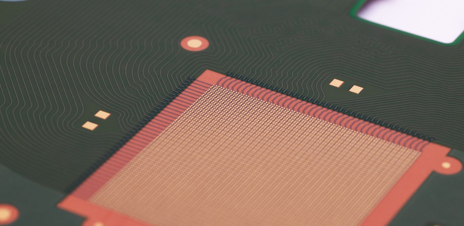
4-Layer Ultra HDI flex, ENEPIG (NiPdAu)
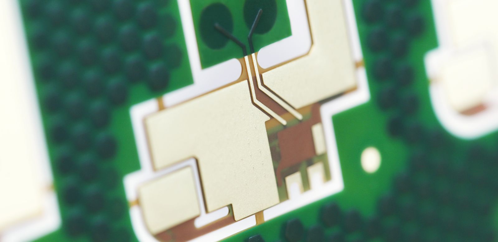
4-Layer highly miniaturized flex , ENEPIG (NiPdAu)
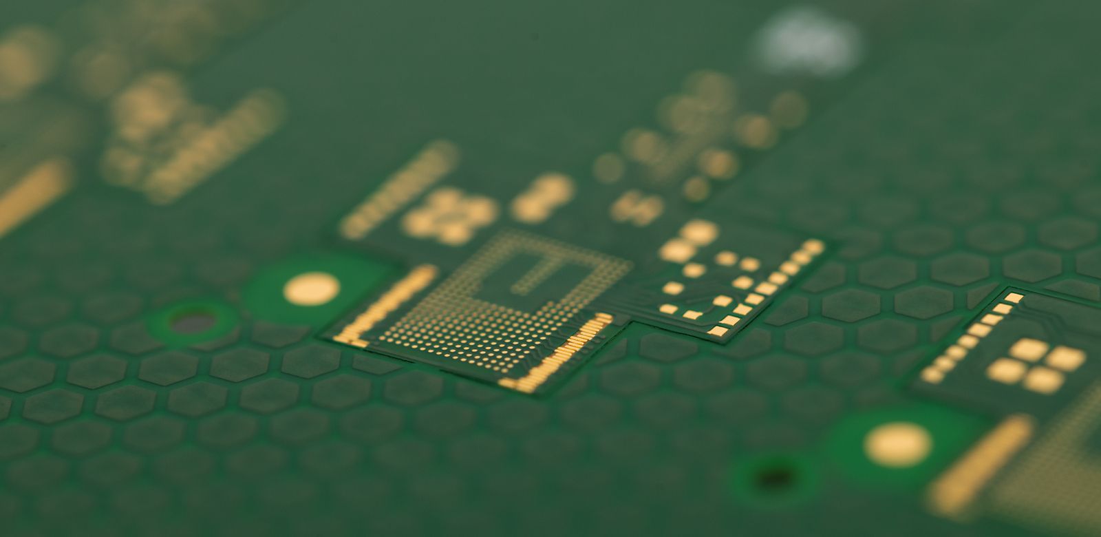
4-Layer ULTRA HDI flex, ENEPIG (NiPdAu)
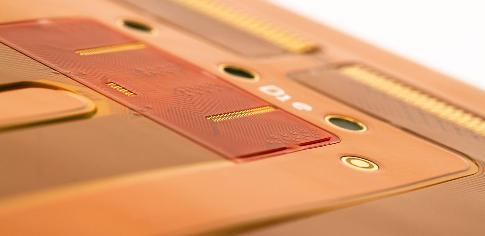
2-Layer flex, ENEPIG (NiPdAu)
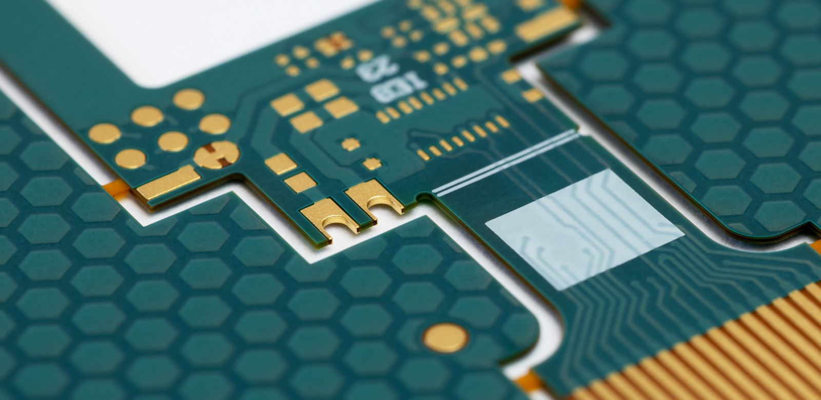
4-Layer ULTRA HDI Edge Plating, ENEPIG (NiPdAu)
Flexible PCBs
Flexible printed circuit boards (FPCs) offer the highest level of 3D miniaturization. Very low bending radii in combination with ultra fine lines enable our customers to build increasingly smaller and highly integrated devices.
Eurotronics and it’s partner production facility have been in this field for many years and manufacture flexible circuits up to 8 layers!
We are working with polyimide foils as thin as 12.5 µm and adhesive bond plies starting at a thickness of 12.5 µm. State of the art equipment enables us to produce FPCs with high output, reliability and repeatability. Depending on the dielectric thickness, laser drilled blind via’s can be as small as 35 µm in diameter and filled with copper in the subsequent plating process to support the use of stacked or staggered via’s and via-in-pad structures.
High-end alignment tools make it possible to achieve very small annular rings and solder mask registration even on extremely complicated multilayer FPCs. As an option, also cover layer foils can be used.
High accuracy laser contour cutting & optimized the space utilization make it possible to achieve excellent 3D miniaturization for small wearable (medical) devices as well as high signal density COF (chip on flex).
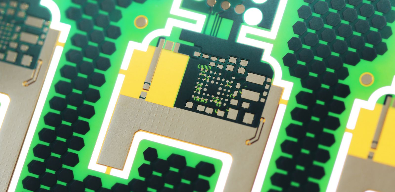
- High-density interconnects (HDIs)
- 1-8 layer flexible PCBs
- Circuit board structures down to 25μm
- Laser micro via’s down to 35μm diameter
- Annular rings down down to 50μm diameter
- Copper filled blind via’s
- Stacked & staggered micro via’s
- Copper thicknesses down to 9µm~12.5μm
- Complex contours and depth milling
- Laser cavities
- Edge plating
- Panel and reel-to-reel production
- Extensive portfolio of surface finishes for all assembly methods
High Density Interconnect flex circuits offer designers the same benefits of flex circuits—smaller, more reliable products—except at a higher level. In addition to the design benefits of HDIs and micro-via’s listed below, HDI circuits give you more design, layout and construction options helping you finish your design in less time.
Lower cost and smaller size – increased circuit density can eliminate extra layers and save up to 40% compared to non-HDI designs.
Use advanced component packaging – high-I/O and fine-pitch feature capabilities possible with HDI.
More design options and flexibility – blind and buried micro-via’s allow for conductor routing on the internal layers under via’s, creating more usable design space per layer.
Improved electrical performance and signal integrity – micro-via’s in high-speed circuits improve electrical performance by allowing shorter circuit paths, stub reduction and lower cross talk and noise.
Improved thermal performance and reliability – micro-via’s lower the z-axis thermal stresses between adjacent layers.
Improved cost effectiveness – Intelligent panel size maximizes circuit density to increase the efficiency of your assembly process.