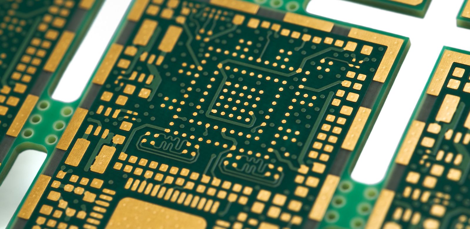
10-Layer AnyLayer HDI, Via-in-pad design
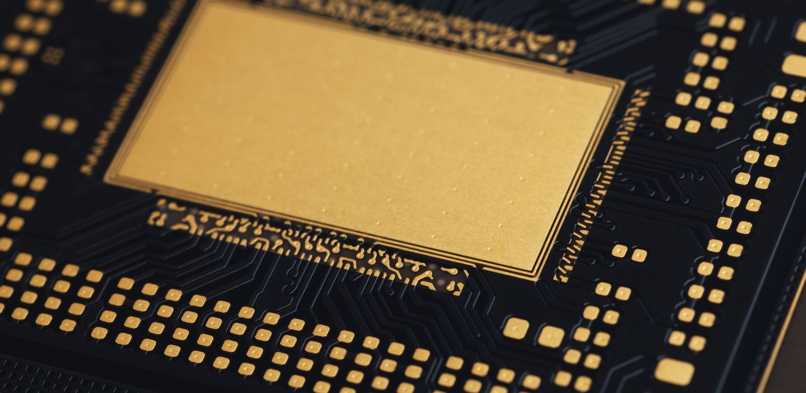
6-Layer HDI, ENEPIG (NiPdAu) for AU Wire bonding
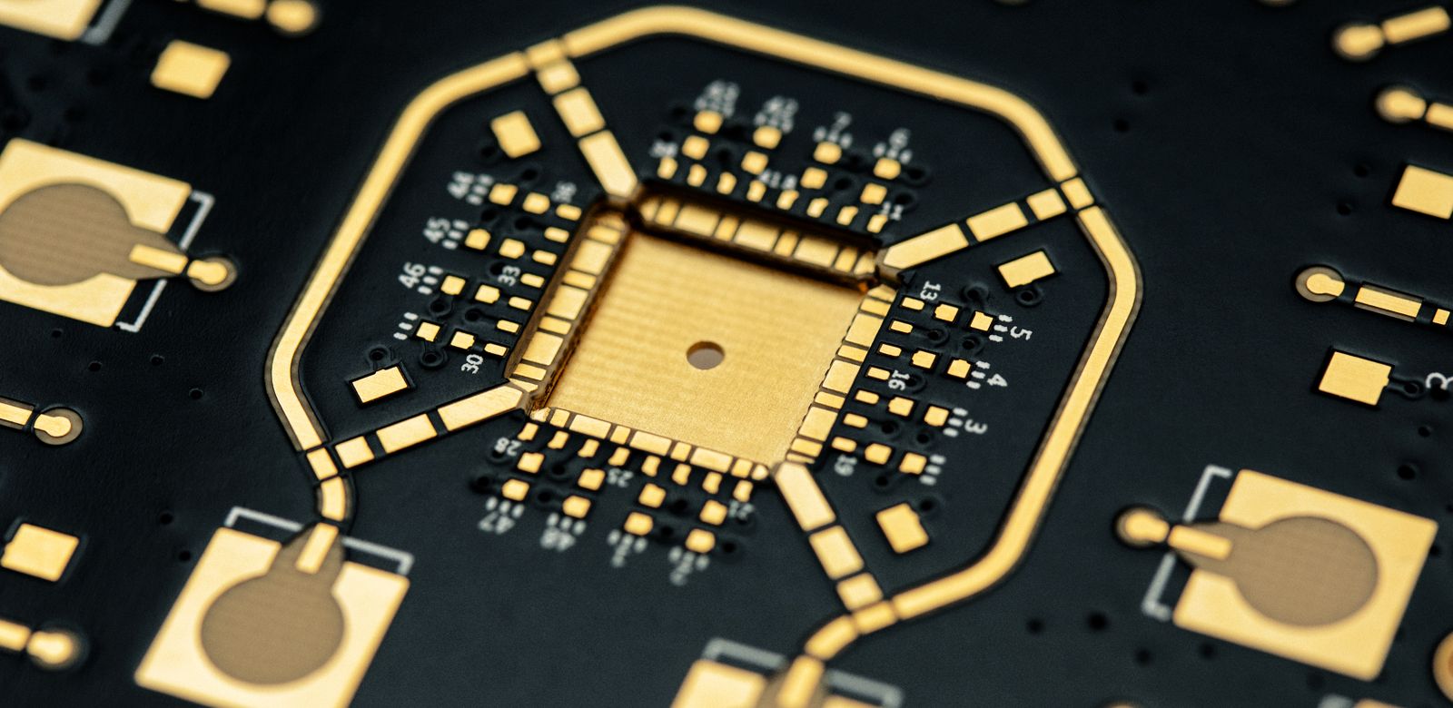
6-Layer HDI, double cavity, ENEPIG (NiPdAu)
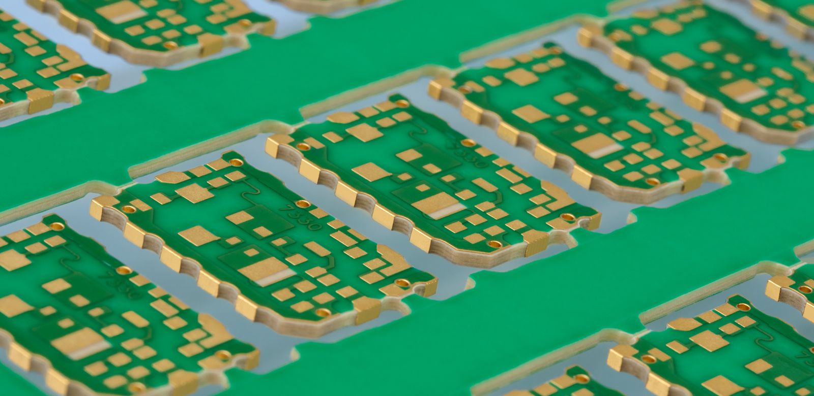
2-Layer RO4003, edge plating
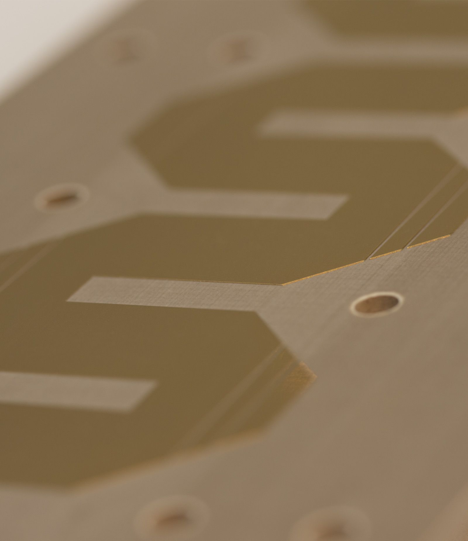
Rogers TC350 Microwave design, ENEPIG (NiAuPd)
Rigid PCBs
Eurotronics and its partner production facility offer rigid PCBs up to 30 layers or more with a clear focus on miniaturization.
Rigid PCBs are available in many different varieties, going from simple single-sided boards to highly integrated multilayer substrates with blind and buried via’s. An even higher degree of integration can be achieved by using the via-in-pad technology – a combination of copper filled via’s with sequential build-ups and stacked or staggered micro-via’s.
Eurotronics offers a wide variety of special (high-frequency) materials and (ultra) thin high-end FR4 base materials, with anti-CAF and low CTE (Z-axis) of 2.4%, to minimize the CTE mismatch.
Additional functionality can be integrated by using special production methods such as hybrid stack-ups, high precision depth milling or cavity designs, edge metallization etc.
The utilization of these state-of-the-art design features is maximizing the design freedom and is one of the key factors for miniaturization.
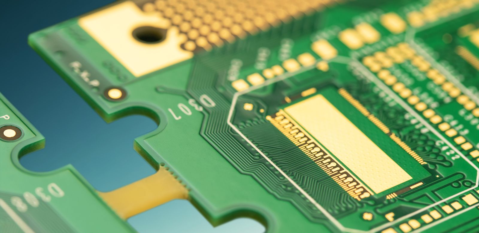
In order to achieve a densely integrated substrate with high reliability, most of our HDI designs are being manufactured in PVA-Technology, using copper filled via’s and sequential build-ups.
- Up to 30 layers
- Maximum board thickness 3.0mm
- Laser direct imaging (LDI)
- Circuit structures down to ≤50μm
- Via-in-pad design
- Laser micro-via’s down to 50μm
- Mechanical via’s down to 100μm
- Copper & resin filled blind via’s
- Stacked & staggered micro-via’s
- ELIC design
- Controlled impedance +/-5%
- Extensive portfolio of surface finishes
Using state of the art equipment makes it possible to build the most challenging designs.
- Mixed dielectric or hybrid stack-ups
- Multiple cavity PCBs, plated or non-plated
- Edge plating
- Castellations
- Metal core & Metal back PCBs for heat-management
- Embedded copper coin
Eurotronics provides wide range of high frequency printed circuit boards whether or not combined with HDI technology and hybrid stack-ups.
- Technological advantage, owing to the experience of our specialists and their wide-ranging knowledge of products and markets.
- Flawless PCBs, as these are manufactured on the most modern systems with the tightest manufacturing tolerances
- Consulting for cost-optimizing panelization design
High frequency PCBs of course come with very specific PTFE based substrates or other. Basically any type of material is available upon request. We regularly work with materials from Rogers, Arlon, Isola I-Tera etc.